Förderjahr 2022 / Projekt Call #17 / ProjektID: 6274 / Projekt: fast_open_switch
A memory controller is a gateware which takes indiviual bytes from the CPU or a DMA engine and puts each byte into a memory module where the data can be retrieved later.
DDR memory is used by almost any IT system to hold massive amount of data for very fast access. Memory modules implement diffferent interface standards. The fastest, largest and most expensive memory modules are DDR5 modules, used in high end graphcis cards with almost 1 TByte/sec data throughput. PCs and Laptops currenlty use DDR4 memory modules as their main memories with capacities up to 32 GByte. Cheap embedded system use the DDR3 standard. We implement DDR3 as FPGAs are mainly used in embedded solutions and those systems do not have any need for extreme large capacities.
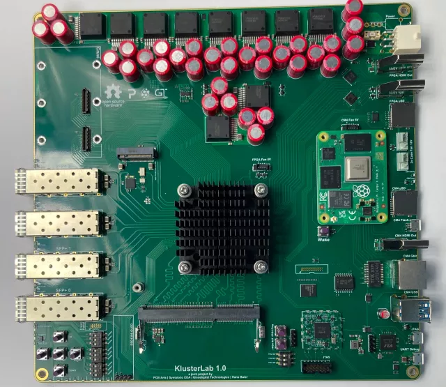
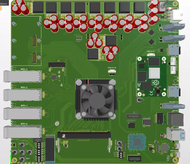
Memory modules in embedded systems do have different layouts and come in different mounting options. We opted for a SODIMM module as it allows us to use memories from different manufacturers. That is important as memoried differ in their timing behaviour. In fact we changed our first module for a module from a different manufacturer which came with better documentation.
Our Vivado simulations with 400MHz DDR3 clock:100MHz controller clock (the same DDR3 clock frequency of what we are running right now at the board) shows that our memory controller can do a burst write at an average of 10.5ns per request (the clock period is 10ns but since there are refreshes every 7.8us, it's now averaging at 10.5 ns). The same rate applies with a burst read. With 512 bits per request (64 Bytes), this makes it around 6GBytes/sec. This is the memory access pattern we expect to see when storing Ethernet packets in memory for later forwarding. With pseudorandom data, it has to do precharge-activate-r/w for some requests so on average it's 48ns per request. With 512 bits per request (64B),this makes it around 1GBytes/sec.But if the request is intentionally forced to change row address per request, the precharge-activate-r/w must now happen per request. On average it's 85ns per request. With 512 bits per request (64B), this makes it around 752MBytes/sec. So we are very happy with the current performance which of course can be further improved later.
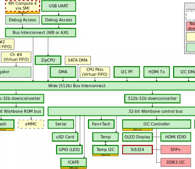
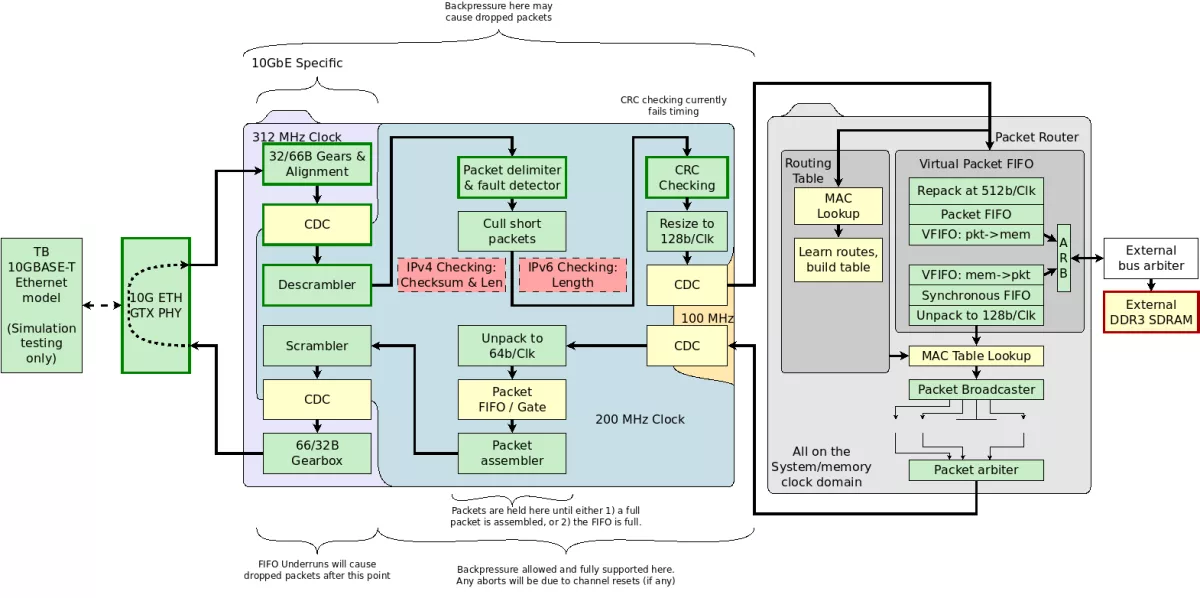
The following graphic shows the architecture of our switch gateware design which we hope to test for function with two 10 Gbit Ehtenrent cards in PCs in the comming weeks.
This open source networking platforn can be the basis for many advanced networking reserach projects.
Ende
Edmund Humenberger